
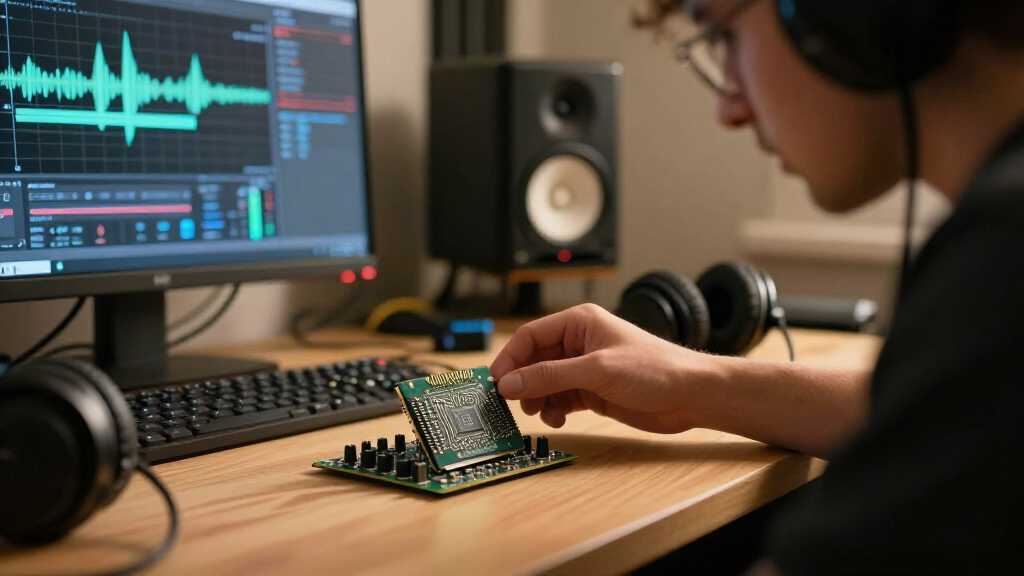
🔍 Read the full analysis: How To Understand The Layers Inside An AI Chip on ThorstenMeyerAI.com

Get audio and creator gear delivered free with Prime
- Fast, free delivery on millions of items
- Prime Video, Amazon Music and more included
- Member-only deals all year
TL;DR
A November 22 explainer from ThorstenMeyerAI.com describes modern AI accelerators as multi-chip packages, not single pieces of silicon. It traces the package from substrate and interposer to compute dies, stacked HBM memory and liquid cooling, then shows how 72-GPU systems are assembled into racks. The article identifies memory bandwidth and advanced packaging capacity as constraints, while some future supply and performance claims remain manufacturer projections.
ThorstenMeyerAI.com published an explainer November 22 showing how current AI accelerators combine compute dies, stacked memory, silicon interposers, substrates and liquid cooling rather than relying on one chip alone. The account matters because it connects hardware performance and availability to memory bandwidth and advanced packaging capacity, as well as to the number of accelerators a data-center rack can hold.
The article uses 3D models to lay out accelerator components in their physical order, while saying the models use schematic dimensions. It notes that Nvidia and AMD do not publish the dimensions of the specific dies, packages or memory stacks described, so the model does not estimate those measurements.
At the bottom is a package substrate, a multilayer base that carries power and signals. Above it, a silicon interposer provides dense connections among compute dies and memory. The article describes high-bandwidth memory, or HBM, as DRAM chips stacked over a base die and linked vertically by through-silicon vias. A cold plate sits above the components to carry liquid cooling.
The examples differ by manufacturer and product. Nvidia says its Rubin GPU has two reticle-limited compute dies and 336 billion transistors; AMD says the MI350 Series integrates eight accelerator complex dies and two I/O dies, with the MI355X at 185 billion transistors. Those figures are manufacturer specifications cited by the article, not independent measurements. The article also describes Nvidia’s GB200 and GB300 NVL72 systems as racks with 72 GPUs and 36 CPUs.
Packaging Sets the Hardware Limits
The physical arrangement helps explain why adding more compute transistors does not, by itself, determine how quickly an AI system can run. The article says compute dies depend on nearby memory and the connections between them; memory bandwidth affects how quickly data reaches the processors. It cites Nvidia product-page figures showing bandwidth rising from 900 GB/s for the V100 to 19.2 TB/s for Rubin. These are product specifications across different generations, not a controlled comparison of real-world model performance.
Packaging also has a production dimension. Silicon interposers connect components with many more wires than a conventional circuit board can support, but manufacturing large, complex packages takes specialized capacity. That makes packaging a potential constraint alongside the supply of compute chips and memory. For buyers, those constraints can affect how many systems are available and their cost; the article does not quantify a resulting price change.
The rack view makes the scale clearer. A single package is only one part of a system that also needs CPUs, switches, power equipment and cooling. Nvidia lists 120 kW of cooling capacity for the GB200 NVL72 rack, illustrating the infrastructure required to operate a high-density deployment. That figure is a specified capacity, not a statement that every rack continuously draws that amount.
Products Worth Considering

LG UltraGear 34-Inch Curved QHD Gaming Monitor, 160Hz, FreeSync Premium

Apple Watch Series 12 GPS 42mm Smartwatch

LG 27GS60QC-B Ultragear 27-inch Curved Gaming Monitor (QHD, 180Hz, 1ms, 1000R)
As an affiliate, we earn on qualifying purchases.
From Silicon Interposer to Rack
The article places its examples in a wider shift toward larger and more vertically integrated packages. It explains that a lithography scanner prints chips within a maximum exposure area called a reticle. TSMC describes its CoWoS-S interposer as supporting an area up to about 2,700 square millimeters, or 3.3 times reticle size. For larger designs, CoWoS-L connects smaller silicon bridges within a carrier layer.
According to the article, TSMC said on October 15, 2026, that it was in real-world production of a five-reticle-size package and working toward nine- and 14-reticle sizes. The article also cites AMD’s statement that its MI455X and MI450X use CoWoS-L. These are company statements about manufacturing and product designs; the explainer does not independently verify production volumes or deployment schedules.
HBM is also evolving vertically. The piece cites SK hynix on stacking 12 layers of 3GB DRAM chips at the thickness of an earlier eight-layer product, and Samsung on a seven-micrometer gap in its 12-high HBM3E. JEDEC’s HBM4 standard, published in April 2025, allows stacks of four, eight, 12 or 16 layers and up to 64GB per stack. The source describes Nvidia’s GB200 and GB300 racks as containing 18 compute trays, nine NVLink switch trays and other management and power equipment.
Supply and Product Details Still Developing
The article does not provide independently verified measurements of die or package dimensions, nor does it quantify how much packaging capacity is available relative to demand. The model’s sizes are schematic, and the article says manufacturers have not published the dimensions needed to make it to scale.
SK hynix’s forecast that demand will exceed supply “through 2030” is a company expectation. The article does not establish how large any shortfall will be, how it might change over time, or what it will mean for particular customers and prices. Product specifications also do not, on their own, establish how a deployed system performs on a given workload.
The source says Nvidia lists the Vera Rubin NVL72 as available now, with 72 Rubin GPUs and 36 Vera CPUs. It does not give independent confirmation of shipment volumes, customer deployments or the configuration’s performance in operation.
Watch Packaging and HBM Capacity
The next developments to watch are manufacturer updates on HBM supply, advanced packaging output and product availability. TSMC’s stated work on larger CoWoS-L packages and the move to taller HBM stacks may shape what future accelerator systems can contain, but the source gives no dates or volumes for those changes beyond the claims cited.
For a clearer picture of deployment, readers will need confirmed shipment figures, system-level performance results and details on how much power and cooling installed racks use in practice. Until those are available, the explainer provides a structural guide to the hardware and its stated specifications rather than a measure of actual market supply or operating performance.
Key Questions
Is an AI accelerator one chip?
Not necessarily. The examples in the article combine compute dies, memory stacks and other components in one package, connected by an interposer and mounted on a substrate.
What does HBM mean?
HBM stands for high-bandwidth memory. It consists of DRAM layers stacked above a base die and connected vertically by through-silicon vias, according to the article.
Why does the interposer matter?
The silicon interposer provides dense connections between compute dies and memory. Its size and manufacturing requirements make advanced packaging capacity part of the supply picture.
How many GPUs are in an NVL72 rack?
The article says Nvidia’s GB200 and GB300 NVL72 rack configurations contain 72 GPUs and 36 CPUs, alongside switch trays, power equipment and cooling infrastructure.
Does the article show exact chip dimensions?
No. Its 3D models show the layers and their order with schematic sizes. The article says the manufacturers do not publish the specific dimensions needed for a scale model.
Source: ThorstenMeyerAI.com